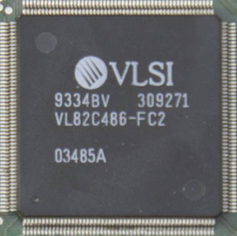
Description:
VL82C486 SC486 Controller
The VL82C486 Controller is designed to perform in 486DX- or 486SX/487SX-based PC/AT- compatible systems running up to 33 MHz.
The VL82C486 replaces the following devices on the motherboard:
- Two 82C37A DMA controllers
- Two 82C59A interrupt controllers
- 82C54 timer
- 74LS612 memory mapper
- 82284 clock generator and ready interface
- 82288 bus controller
The controller also includes the following:
- Memory/refresh controller
- Port B and NMI logic
- Bus steering logic
- Turbo Mode control logic
- Parity checking logic
- Parity generation logic
- Support for Weitek numeric coprocessors.
The memory controller logic is capable of accessing up to 64 MB. There can be up to four banks of 256K, 1M, or 4M DRAMs used in a system. The VL82C486 can drive four banks without external buffering. Built-in Page Mode operation and up to four-way interleaving allows the PC designer to maximize system perform- ance using low-cost DRAMs. Programmable DRAM timing is provided for RAS precharge, RAs-to-CAS delay, and CAS pulse width.
Support for write-through cache controllers is provided through the use of a -MISS pin to detect cache-hits and cache-misses.
The VL82C486 can be programmed to generate the ISA bus timing from the CPU clock oscillator or a separate asynchronous oscillator.
The VL82C486 also performs all the data buffer control functions required for a 486XX processor-based PC/AT system. Under the control of the CPU, the VL82C486 routes data to and from the CPU's D bus, the internal XD bus, and the slots (SD bus). During CPU ISA bus reads, the data is latched for synchronization with the CPU. Parity is checked for D bus DRAM read operations. The chip does not generate parity for CPU writes to DRAM.
Features:
- Fully compatible with 486-based PC/AT systems
- Up to 33 MHz CPU operation
- Replaces the following peripheral logic on the motherboard:
- Two 82C37A DMA controllers
- 74LS612 memory mappers (extended to support 64 MB)
- Two 82C59A interrupt controllers
- 82C54 timer
- 82284 clock generator and ready interface
- 82288 bus controller
- Includes:
- Memory/refresh controller
- Port A, B, and NMI logic
- Bus steering logic
- Parity generation/checking for on-board DRAM
- Turbo control
- Hidden off-board, stolen on-board refresh
- Staggered RAS refresh
- Three-stateable outputs for board testing
- Memory controller features include:
- Page Mode DRAM access
- One to four banks 32 bits wide
- One or two banks 64 bits wide
- Two- or four-way interleave support
- Programmable RAS#/CAS# timing
- Burst support
- Supports:
- Up to 64 MB system memory
- 256K, 1M or 4M DRAM
- Double-sided SIMMs
- Secondary cache interface
- 8- or 16-bit wide BIOS ROM
- Shadow RAM in the 640K-1M area
- Asynchronous ISA bus operation up to 16 MHz
- Relocation of slot ROMs
- Power saving features include:
- Sleep Mode
- Slow DRAM refresh
- Other features:
- Programmable for 10- or 16-bit internal I/O addressing
- Programmable drive on the DRAM and ISA bus signals
- Programmable memory access to define "fast-bus", local bus, slot bus, non-cacheable and write-protect areas
- Input pin defines access to local bus devices
- 1.0-micron CMOS technology
- 208-lead MQFP (metric quad flat pack)
Disclaimer
The info found in this page might not be entirely correct. Check out this guide to learn how you can improve it.
 Image 1 of 1 (Nexus 6)